COLLECTED BY
Organization:
Internet Archive
The Internet Archive discovers and captures web pages through many different web crawls.
At any given time several distinct crawls are running, some for months, and some every day or longer.
View the web archive through the
Wayback Machine.
Web wide crawl number 16
The seed list for
Wide00016 was made from the join of the top 1 million domains from CISCO
and the top 1 million domains from Alexa.
TIMESTAMPS
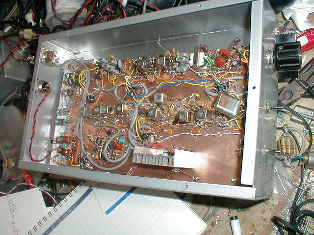
14MHzSSB10mW transceiver
The reason of this events: The reason of this production is very simple.
I wanted to QRV on 14MHz SSB mode. One day when I walking on Akihabara
city in Tokyo , while I have heard the sample transceiver on the ham shop
,I have known that 14MHz can be used for domestic communication. They made
Japanese domestic QSO about 14.18MHz.
The whole Construction : You can call the transceiver like this as "OZL
type". Characteristics of the "OZL type" are as follows.
1. Single conversion super.
2. Using two DBM-s as modulator and converter.
3. Modulator DBM is used as demodulator in receiving time.
4. All amplifiers are used in transmitting and receiving time.
5. Case is second use of my failed or useless machine.(This time I used
my useless old 10W 7MHz transmitter.)
6. All decals are done with the "Magic ink". Very simple way!
7. Normal "OZL type" uses 12V DC power from cigar lighter of
the car. But in this machine I used 20V DC from my DC power supply. The
reason of my choosing high voltage are as follows. One reason is in order
to press the variable capacitor of the VXO oscillator for it's minimum
capacitance and to get the highest frequency and to get the wide frequency
range of the operation. Second reason is to use 24V relays instead of 12V
relays. I got these 24V relay with only 10 dollar for 10 peace. It was
cheep Junk but super micro molded type can be used for 430MHz. The name
of these relays are G6H2-24V. Maker is OMRON company. Third reason of high
voltage is in order to get 10W power easy with good linearity. In my experience
it is difficult to get 10W with 12V power pupply.
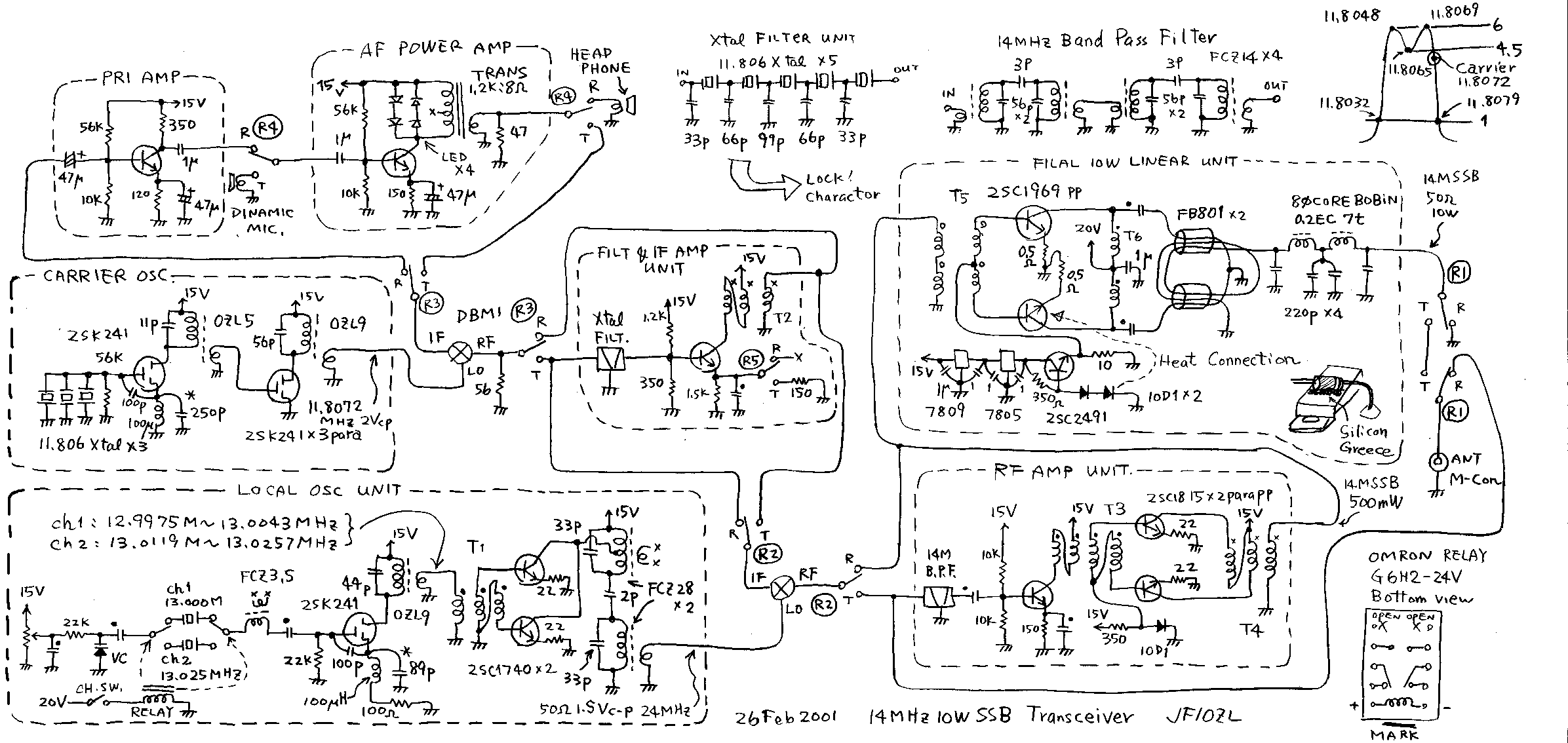
Explanation of the circuit diagram:
1. The black circle marked capacitor is 0.01 micro F ceramic capacitor.
2.You should adjust the snow marked two capacitors on the oscillators to
be got the maximum each output power.
3. All NPN transistors who has no mark are 2SC1815. Maker: Toshiba. Usage
:signal amplifier. Pc=0.4W, Vcbo=60V, Hfe=70 to 700, ft=80MHz.. I show
you the character of another transistors as follows. 2SC1815:maker=Toshiba:usage=amp:Pc=0.4W:Vcbo=60V:Hfe=70to700:ft=80MHzmin///
2SC1740:maker=Rohm:usage=universalamplifier:Pc=0.3W:Vcbo=50V:Hfe=120to820:ft=180MHz///
2SC2491:maker=Sanken:usage=powersalamplifier,switching:Pc=50W:Vcbo=100V:Hfe=unknown:ft=30MHz///
2SC1969:maker=Toshiba:usage=CB bandRFpoweramplifier:Pc=20W:Vcbo=60V:Hfe=unknown:ft=unknown,
(Po=18W,at27MHz,Vcc=12V,Pi=1W)
4. FET used on carrier oscillator is 2SK241. Maker Toshiba. Mos FET. Usage
=FM VHF amplifier. Id=30mA, Pc=200mW, Idss=1.5 to 14mA, gm=10mS, Crs=0.035pF,
PG=28dB on 100MHz.
5. FIve micro relays named "G6H2-24V" are used as switching the
connection of the circuit, from receiving to transmit. This relay is made
by Omuron Co,. in Japan.
6. T1,T2,T4 are FB801 tri -filer 2turn with 0.2mm diameter enamel wire.
7. T3 and T5 are FB801 deca-filer 2 turn. Deca filer means the transformer
made with four wires.
8. T6 is FB801 double filer 2 turn. Double filer means the transformer
made with two wires.
9. Low pass filter are made with the coils "8.0mm diameter bobbin,
0.2mm EW 7 turn." This is designed as a Pie type low path filter with
Q=1 frequency is 14MHz.
Block diagram of trnsmitter
signal flows left to right
dinamic
microphone |
audio
amp |
DBM1
as
modulator |
11.806Mhz
DSB
signal |
crystal
filter makes it
to LSB
|
IF
AMP |
DBM2
as
convertor |
14MHz
USB |
14MHz
BPF |
3stage
HF
AMP |
LPF |
ANT
14MHz
USB
10W |
|
|
upper |
|
|
|
26MHz
go upper |
|
|
|
|
|
|
carrier
oscillater
11.806MHz |
buffer AMP |
|
|
2channel
VXO
13MHz |
pusu-pusu
doubler |
|
|
|
|
|
Signal flow on transmitting time:
1. I use 600 ohms dynamic microphone. It generates 50mVc-p signal with
my voice. This audio A- class amplifier has 30dB voltage gain. Therefore
my voice becomes over1Vc-p signal on it's outside. LED diode clipper is
used to limit the amplitude of the outside of the audio amplifier for 250mVc-p.
LED 's inner impedance become low when its voltage becomes over 2 volts.
Four LED's are connected parallel series. Therefore the amplitude of the
first side of the audio output transformer cannot be 4Vp-p. This audio
signal is used to modulate the carrier in the next stage.
2. Carrier oscillator is constructed with 11.806 named crystal and FET.
It oscillates 11.8072MHz actually. In order to generate the frequency on
the upper slope of the crystal filter , this oscillator shall be tuned
at this frequency. In this case I had to use FET only on this circuit.
With transistor I could not tune the frequency on 11.8072MHz. When I made
D-G pierce oscillator the frequency became higher than 11.808MHz. I changed
the oscillator circuit to G-S pierce circuit. Then it oscillated 11.805
MHz. I changed the two crystals parallel , the frequency became 11.806MHz.
I got 11.8072MHz by connecting three crystals parallel. In order to drive
the double balanced modulator (DBM) as it's requiring local port signal
strength , that is over 1mW, I had to set the buffer amplifier between
the local oscillator and LO port of the DBM. This buffer outputs 2Vc-p
signal. It is enough strength to drive the four diodes of the DBM and not
to be disturbed by the audio signal on RF port of DBM. LO port carrier
signal have to be strong more than 10dB than the modulating signal of RF
port, to ensure the correct action of the modulator. Or else , the modulated
signal becomes " over modulation".
3.Please look another page of my home page about the construction and action
of DBM. Here I used four silicon signal diodes named 1S1588(Toshiba Co,.).
And also I used a pair of ferrite core named FB801, to construct each double
balanced mixers. Here this DBM1 is used as a modulator. Here the 11.8072MHz
CW signal is modulated by the audio signal. On the IF port of this DBM1
happens (comes up) the carrier suppressed double side band signal. You
can see the 56 ohm resister on the IF port of the DBM1. It is used to shorten
the output impedance of this DBM, not to be over 56 ohms. Without this
resistor , the carrier suppression become 20dB worse. With this resister
the carrier suppression are achieved as about -40dB.
4. Because the carrier frequency is located on the upper slope of the pass
band of the crystal filter, only lower side band of the double side band
signal on the IF port of the DBM1 can be pass through crystal filter. Upper
side band signal is rejected to path through the crystal filter.
5. This lower side band signal (LSB) is amplified with the IF amplifier.
The LSB signal came out of this amplifier is 400mVc-p with 50 ohms load.
6. In order to get the wanted 14Mhz USB signal from this 11.8MHz LSB signal,
26MHz CW signal shall be used. The calculation is " 26MhzCW -11.8MHz
LSB=14.2MHzUSB". Please remember that "when the mixer generates
the difference of two input signals, the USB changes LSB, LSB changes USB",
and, " when the mixer generates the sum of the two input signals ,
USB became from USB, LSB became from LSB". I have about 5 kg of crystal
( several hundred). I chose from this stock the crystal named 13.025MHz.
With this crystal VXO ( crystal controlled frequency tunable oscillator)
is constructed. It generates from 13.0119 to 13.0257 MHz. This signal is
doubled with a push - push doubler. The output of this buffer amplifier
is from 26.023 to 26.0514MHz1.5Vc-p CW signal with 50 ohms load. This signal
drives the LO port of the DBM2.With This local signal I can make 14.2166
to 14.2442MHz as it's transmitting frequency. Yes It can be used on the
SSB band. But I want to make about 14.18MHz in order to get many chance
to meet the Japanese domestic stations. Therefore I requested to ham shop
to send me 13.000MHz crystal. With using this crystal, I could oscillate
12.9975 to 13.0043MHz. I can QRV from 14.1878MHz to 14.2014MHz with this
crystal as indicated channel one on the circuit diagram.
7. On the DBM2 , 26MHz CW and 11.8MHz LSB signal is mixed. And the 14.2MHz
USB signal is obtained(got) on the RF port of the DBM2. Here the signal
rebels of the local port and IF port shall be compared. Anytime the LO
port shall be driven stronger then IF port more than 10dB.
8. Already I got 14.2MHz USB signal. This signal is amplified by the Radio
frequency (RF) amplifier unit. The first step of the RF amplifier is made
of A class single amplifier. The second step of the RF amplifier is constructed
by the B- class push- pull amplifier. In order to stabilize the bias of
final amplifier the power diode 10D1 is used with a 30mA of bias current.
Here shall not to be used the small signal silicon diode like 1S1588. Please
remember that " With more current on the bias diode, more stable of
the bias circuit is achieved". T3 is made from four wire transformer.
Instead of T3, two tri- filer transformers can be used. But T3 is more
save resources type. ( But to make such a hand made rig with myself is
not "save resources type action" as itself. Anyway the amateur
radio is the "King's hobby", effective only to spend money and
time)....On the front of the RF AMP unit , the 14MHz band pass filter is
located. This filter reject to income some unwanted signals coming to RF
AMP unit. On the end of the RF AMP unit, 14MHz low pass filter is located.
It prevents to go out the unwanted harmonized signal born in RF AMP unit.
Without this filter , this rig may cause the TVI , we call "I- chen"
in Japanese. This filter is required by the government to allow to use
the rig as a machine of amateur radio.
Block diagram of receiver
signal fows left to right
ANT
14MHZ
USB |
14MHz
BPF |
2stage
HF
amp |
DBM2
as
convertor |
11.806Mhz
DSB
signal |
crystal |
IF
AMP |
DBM1
as de-
modulator |
pri
AMP |
AF
AMP |
head
phone |
|
|
|
26MHz
go uppe |
|
|
|
upper |
|
|
|
|
|
2channel
VXO
|
13MHzpusu-pusu
doubler |
|
|
carrier
oscillater
11.806MHz |
buffer
AMP |
|
|
|
Signal flow of the receiving time:
1. The 14MHz USB signal came from the antenna (aerial) is amplified by
the RF amplifier unit.
2. This 14MHz USB signal and the oscillated 26MHz signal are mixed on DBM2.
It products the 11.8MHz LSB signal. We call such a character of DBM to
send a signal from RF port to IF port and from IF port to RF port as "two
way ability". I feel this ward may be English or German originally.
My translation made from Japanese with my sense. I am afraid to make miss
translation.
3. This 11.807MHz signal is amplified by the IF amplifier. You can see
the collector current is reduced when receiving time. Instead of this method
the IF amplifier makes unwanted self oscillation.
4. Also in this receiving time, 11.8072MHZ carrier drives the LO port of
the DBM1. Therefore the carrier suppressed upper side band signal (USB)
on the IF port of the DBM get the carrier again. It becomes the audio signal
on the IF port of the DBM1. This process is called as the demodulation.
5. This demodulated audio signal is amplified by the audio amplifier. And
it is heard with the head phone. In receiving time pri-audio amplifier
is add to audio power amplifier to get more total gain. And the audio is
heard with head phone.
The result of this transceiver:
I made nine QSOs with this rig and 14MHZ dipole antenna on the berranda
of my house about 10M high. Please look the end of this page ! I made contact
with another aria in Japan from my house located in Tsuchiura city. 14MHz
can be used only from 10 o'clock before noon to two o'clock after noon
for domestic communication. But I feel I would have Yagi antenna!!
14mssb10wfh.jpg

14mssb10w.gif

14MHz 10W SSB Transceiver
惢嶌偺棟桼丗崱夞偺惢嶌偺棟桼偼嬌傔偰扨弮偱偡丅廐梩尨偺僴儉僔儑僢僾偱傾儅僠儏傾柍慄偺婡夿傪偄偠偭偰偄偰丄偙偺侾係俵俫倸偑崙嵺僶儞僪偱偁傝側偑傜丄偍拫慜屻偼偳偆傗傜崙撪偺俻俽俷偵傕巊偊傞傜偟偄帠偑傢偐偭偨偺偱丄嶌偭偰傒傑偟偨丅
慡懱偺峔惉丗崱夞傕庤姷傟偨乽俷倅俴曽幃乿偡側傢偪丄慡偰偺夞楬傪憲庴怣嫟梡偱巊梡偟偰丄儕儗乕偱愗傝懼偊傞曽幃傪偲傝傑偟偨丅崱夞偙偺婡夿偼屌掕偱偺傒
巊梡偡傞慜掱乮堏摦偱侾係俵偺傾儞僥僫傪忋偘傞偺偼偪傚偭偲戝曄偦偆乯側偺偱丄揹尮偼壠乮偆偪乯偺埨掕壔揹尮偺嵟戝揹埑偱偁傞俀侽倁偱愝寁偟傑偟偨丅
俀侽倁偲崅偔愝掕偡傞帠偵傛偭偰丄幵偺僔僈儔僀僞乕偐傜揹尮傪嫙媼偟偰堏摦塣梡偱偒傞壜擻惈偑柍偔側傞偲偄偆僨儊儕僢僩偑偁傝傑偡偑丄媡偵壓婰偺俁偮偺儊
儕僢僞偑摼傜傟傑偡丅?@奜晹偐傜嫙媼偟偨俀侽倁傪俈俉侾俆偱侾俆倁偵埨掕壔偟偰嶌偭偨撪晹埨掕揹尮揹埑偱僶儕僢僉儍僾偺梕検嵟彫偵側傞傑偱丄偠傘偆暘偵
僶儕僉儍僢僾傪峣傝忋偘偰偮偐偊傞偺偱丄倁倃俷偺壜曄斖埻偑峀偑傝丄寢壥偲偟偰僶儞僪撪偱偺僇僶乕斖埻偑峀偘傜傟傞丅乮屻偱徻嵶愢柧偟傑偡乯?A侾俀倁儕
儗乕偼梡搑偑峀偄偺偱廐梩尨偱傕侾屄俁侽侽墌掱搙偡傞偑丄偙偙偱偼恖婥偑柍偄暘埨偔丄侾侽屄侾侽侽侽墌偱擖庤偱偒偨丄俧俇俫俀亅俀係倁偺僗僩僢僋傪巊梡偱
偒傞丅?B揹尮揹埑偑崅偄曽偑丄僼傽僀僫儖偺憹暆婍偺弌椡揹椡偑弌偟傗偡偄丅懠偺儁乕僕偱傕尵偭偰傑偡偑丄揹尮侾俀倁偱侾侽倂弌偡偺偼丄寢峔擄偟偄偱偡丅
巹
偺宱尡揑偵偼丄偼偄丅働乕僗偼奧晅偒傾儖儈僔儍乕僔乕偱偡偑丄偄傑偐傜侾侽擭慜偵嶌惉偟偨丄俈俵俫倸俽俽俛憲怣婡偺暔傪丄夡偟偰巊偄傑偟偨丅
夞楬恾偺愢柧丗
侾丏 仠偺婰崋偺僐儞僨儞僒乕偼丄侽丏侽侾兪俥偺僙儔儈僢僋僐儞僨儞僒乕丅
俀丏 擇偮偺敪怳婍偺乮仏乯儅乕僋偺婣娨僐儞僨儞僒乕偼丄敪怳弌椡嵟戝偲側傞條偵丄偤傂偙傑傔偵挷惍偟偰梸偟偄強丅
俁丏
恾偺拞斣崋婰嵹柍偄偺俶俹俶僩儔儞僕僗僞乕偼丄慡偰俀倱們侾俉侾俆丅庡梫彅尦丗儊乕僇乕丗搶幣丅斈梡彫怣崋憹暆梡丅俹們亖侽丏係倂丅倁們倐倧亖俇侽倁丅
俫倖倕亖俈侽乣俈侽侽丅倖倲亖俉侽俵俫倸丅懠偺僩儔儞僕僗僞乕偺彅尦傕壓婰偵帵偟傑偡丅
2SC1815:maker=Toshiba:usage=amp:Pc=0.4W:Vcbo=60V:Hfe=70to700:ft=80MHzmin///
2SC1740:maker=Rohm:usage=universalamplifier:Pc=0.3W:Vcbo=50V:Hfe=120to820:ft=180MHz///
2SC2491:maker=Sanken:usage=powersalamplifier,switching:Pc=50W:Vcbo=100V:Hfe=unknown:ft=30MHz///
2SC1969:maker=Toshiba:usage=CB bandRFpoweramplifier:Pc=20W:Vcbo=60V:Hfe=unknown:ft=unknown,
(Po=18W,at27MHz,Vcc=12V,Pi=1W)
係丏 僉儍儕傾乕敪怳婍偺俥俤俿偼丄俀倱倠俀係侾丅庡梫彅尦丗儊乕僇乕丗搶幣丅俵俷俽俥俤俿丅俥俵丆倁俫俥憹暆梡丅俬倓亖俁侽倣俙丅俹們亖俀侽侽倣倂丅俬倓倱倱亖侾丏俆乣侾係倣俙丅倗倣亖侾侽倣俽丅俠倰倱亖侽丏侽俁俆倫俥丅俹俧亖俀俉倓俛乮侾侽侽俵俫倅乯
俆丏 憲庴怣愗傝懼偊偼挻彫宆儕儗乕丄僆儉儘儞惢偺俧俇俫俀亅俀係倁乮俀係儃儖僩丄俀夞楬乯傪俆屄巊梡偟偰偄傑偡丅
俇丏 俿侾丆俿俀丆俿係偼丄俥俛俉侽侾偵侽丏俀倣倣僄僫儊儖儚僀傾傪僩儕僼傽僀儔乮俁杮潃傝姫乯俀倲丅
俈丏 俿俁丆俿俆偼俥俛俉侽侾偵侽丏俀倣倣僄僫儊儖慄傪僨僇僼傽僀儔乮係杮傛偠傝姫乯俀倲丅
俉丏 俿俇偼丄俥俛俉侽侾偵侽丏俀倣倣僄僫儊儖儚僀傾傪僟僽儖僼傽僀儔乮俀杮傛偠傝姫乯俀倲丅
俋丏 僼傽僀僫儖偺屻傠偺兾宆儘乕僷僗僼傿儖僞乕偺僐僀儖偼俉丏侽倣倣捈宎偺僐傾擖傝儃價儞偵侽丏俀倣倣儚僀傾俈倲丅乮兾宆儘乕僷僗僼傿儖僞乕偼丄俻亖侾丆廃攇悢侾係俵俫倸丆僀儞僺乕僟儞僗俆侽僆乕儉偱愝寁丄俠俻弌斉幮乽僩儘僀僟儖僐傾妶梡昐壢乿傪嶲徠乯
僽儘僢僋僟僀傾僌儔儉
憲怣帪
僟僀僫
儈僢僋
儅僀僋仺 |
俙俥
僷儚乕
傾儞僾仺 |
僟僀僆乕僪
俢俛俵侾
曄挷婍 |
侾侾丏俉侽俇
俵俫倸
俢俽俛怣崋仺 |
悈徎
僼傿儖僞乕偱
俴俽俛怣崋
偵側傞仺 |
拞娫廃攇
憹暆婍仺 |
僟僀僆乕僪
俢俛俵俀
廃攇悢
曄姺婡 |
侾係俵俫倸
倱倱倐怣崋
仺 |
僶儞僪僷僗
僼傿儖僞乕 |
崅廃攇
揹椡
憹暆婍偱
侾侽倂偵 |
俴俹俥 |
傾儞
僥僫 |
|
|
仾 |
|
|
|
仾 |
|
|
|
|
|
|
侾侾丏俉侽俇
俵俫倸
斃憲攇
敪怳婍 |
娚徴
憹暆婍 |
|
|
俀僠儍儞僱儖
侾俁俵俫倸
倁倃俷仺 |
僾僢僔儏
僾僢僔儏
僟僽儔乕
俀俇俵俫倸 |
|
|
|
|
|
憲怣帪偺怣崋偺棳傟
侾丏
巹偼丄僟僀僫儈僢僋儅僀僋乮僀儞僺乕僟儞僗俇侽侽僆乕儉偺傕偺乯傪晛抜巊梡偟偰偄傑偡丅偙傟偵岦偐偭偰榖偡偲丄巹偺惡偼俆侽倣倁們乗倫乮僙儞僞乕僣乕僺乕
僋丟愲摢抣丗埲壓摨條乯偺揹埑怣崋偵側傝傑偡丅僆乕僨傿僆傾儞僾偼偄傢備傞俙媺憹暆婍偱丄揹埑棙摼偑偙傟偩偗偱俁侽倓俛偁傝傑偡丅傛偭偰丄偙偺憹暆婍偺弌
椡偵偼丄壒惡怣崋侾倁們乗倫掱搙偑弌椡偝傟傑偡偑丄憹暆婍偺僩儔儞僗偺侾師懁偵俴俤俢偵傛傞怳暆惂尷偑慻傑傟偰偍傝丄壒惡弌椡怣崋偼俀俆侽倣倁們乗倫偱僋
儕僢僾乮惂尷乯偝傟傑偡丅偙傟偼丄俴俤俢偑弴曽岦揹埑俀倁傪挻偊偨偲偨傫偵揹棳偑側偑傟偰丄岝偩偟丄撪晹掞峈偑彫偝偔側傞偲偄偆摿惈傪棙梡偟偨暔偱偡丅偙
偺丄憹暆偝傟偨壒惡怣崋偼丄戞堦暯峵曄挷婡乮俢俛俵侾乯偺俼俥億乕僩偵擖椡偝傟傑偡丅
俀丏
嬊敪儐僯僢僩偱偼丄侾侾丏俉侽俇偲彂偄偰偁傞悈徎傪巊偭偰侾侾丏俉侽俈侾俵俫倸傪敪怳偝偣偰偄傑偡丅巒傔偙偙偵偼俥俤俿俀俽俲俀係侾偺俢亅俧僺傾僗夞楬傪
偮偐偭偰傒傑偟偨偑丄偳偆偟偰傕廃攇悢偑侾侾丏俉侽俉俵俫倸埲忋偵側偭偰偟傑偄丄僋儕僗僞儖僼僀儖僞乕偺捠夁懷堟忋抂偱偁傞侾侾丏俉侽俈俵俫倸嬤曈偵帩偭
偰偔傞帠偑偱偒傑偣傫偱偟偨丅偐偲偄偭偰丄偦偺偨傔偵悈徎傪拲暥偡傞栿偵偼偄偒傑偣傫乮暿偵乽峴偒傑偣傫乿偲偄偆掱偱傕側偄傫偱偡偑丄偱偒傞偩偗庤帩偪偺
晹昳偱娫偵崌傢偣偨偄偺偑怱忣丅偟偐偟丄媡偵偄偆偲丄乽悈徎傪拲暥偡傞帠傪偨傔傜偭偰偼偄偗側偄丅乿偲傕丄怽偟忋偘偨偄乯丅俧亅俽僺傾僗敪怳婍傪巊梡偟偰
傒偨強崱搙偼掅偔側偭偰侾侾丏俉侽俆俵俫倸傪敪怳偟傑偟偨丅悈徎傪僷儔偵偮側偖偲侾俲俫倸偢偮敪怳廃攇悢偑崅偄曽偵堏摦偡傞偺偱丄俁屄暲楍愙懕偟偨強偱側
傫偲偐栚昗偺廃攇悢偱偁傞丄僋儕僗僞儖僼僀儖僞乕偺捠夁懷堟忋抂侾侾丏俉侽俈俵俫倸嬤曈偵帩偭偰偔傞帠偑偱偒傑偟偨丅偟偐偟丄側偤偐偙偺敪怳婍偺弌椡偼
侽丏俆倁掱搙偲俢俛俵傪捈愙嬱摦偡傞偵偼傗傗晄懌偱偟偨偺偱丄娚徴憹暆婍傪侾抜晅偗傑偟偨丅俧亅俽僺傾僗敪怳婍偼偄偮傕巊偭偰偄傞俢亅俧僺傾
僗夞楬傛傝傕弌椡揹椡偑彫偝偄孹岦偵偁傝傑偡丅偙偺弌椡偼丄侾侾丏俉侽俈俀俵俫倸俀倁們亅倫乮俆侽僆乕儉晧壸乯丄偡側傢偪係侽倣倂亖侾俇倓俛倣側偺偱丄廫
暘梋桾偱僔儕僐儞彫怣崋僟僀僆乕僪乮侾俽侾俆俉俉乯偱峔惉偝傟偨俢俛俵傪嬱摦偱偒傑偡丅傑偨丄壒惡怣崋偺僺乕僋偼丄偝偒傎偳愢柧偟偨條偵俀俆侽倣倁們乗倫
偵墴偝偊傜傟偰偄傑偡偺偱丄嬊敪偲壒惡怣崋偺斾棪偼乮俀倁懳俀俆侽倣倁偱乯俀侽倓俛掱搙妋曐偝傟偰偍傝丄俢俛俵偲偟偰傕朞榓偵傛傞榗傒傪敪惗偡傞帠柍偔摦
嶌偱偒傑偡丅
俁丏
夞楬恾偱俢俛俵侾偲昤偄偨暯峵曄挷婡偵娭偟偰偼丄嶌傝曽媦傃摦嶌摿惈偑巹偺儂乕儉儁乕僕偺暿偺儁乕僕偵愢柧偟偰偁傝傑偡偺偱丄偛棗偔偩偝偄丅偙偙偱偼丄壒
惡怣崋偵傛偭偰僉儍儕傾乕乮斃憲攇乯偱偁傞侾侾丏俉侽俈俀俵俫倸偺怣崋偑曄挷偝傟偰丄俬俥億乕僩偵偼丄斃憲攇梷埑椉懁懷攇乮偼傫偦偆偼傛偔偁偮傝傚偆偦偔
偨偄偼丗俢俽俛乯怣崋偑弌偰偒傑偡丅俢俛俵侾偺俬俥億乕僩偺強偵傇傜偝偑偭偰偄傞俆俇僆乕儉偺掞峈偼堦庬偺僀儞僺乕僟儞僗僋儔儞僾偱偡丅偙傟偑柍偄偲丄
俢俛俵偺弌椡偱偁傞俬俥億乕僩偺僀儞僺乕僟儞僗偑朶傟偰丄惓忢側摦嶌偑弌棃偢偵丄斃憲攇梷埑斾偑埆壔偟傑偡丅嬶懱揑偵尵偆偲丄斃憲攇梷埑斾偑俀侽倓俛掱搙
偵側偭偰偟傑偄傑偡丅偙偺懳嶔偲偟偰晅偗偨暔偱偡丅嶳懞俷俵偑丄変乆偺僶僀僽儖乽僩儘僐傾乿偺拞偱偍偭偟傖偭偰偄傞條偵丄乽俢俛俵偺惓忢側摦嶌傪曐徹偡傞
堊偵偼丄奺億乕僩偵俇倓俛掱搙偺掞峈尭悐婡傪庢傝晅偗傞帠偑棟憐揑乿側偺偱偡偑丄偙傟偱偼揹椡偺柍懯偑敪惗偟傑偡丅昁梫側強偩偗偵嵟掅尷晅偗傞偺偑尰幚揑
偱偟傚偆丅
係丏
偙偺斃憲攇梷埑椉懁懷攇乮俢俽俛乯怣崋偑丄師偺儔僟乕宆俆抜悈徎僼僀儖僞乕傪捠夁偡傞嵺偵丄忋懁懷攇乮倀俽俛乯怣崋偼悈徎僼傿儖僞乕偺捠夁懷堟偐傜偼偢傟
偰偄傞偺偱丄捠夁偱偒傑偣傫丅丄堦曽丄壓懁懷攇乮俴俽俛乯怣崋偼悈徎僼傿儖僞乕偺捠夁懷堟傪捠傞偺偱丄捠夁偱偒傑偡丅寢壥偲偟偰壓懁懷攇乮俴俽俛乯怣崋偩
偗偑偙偙偐傜弌偰棃傑偡丅
俆丏 偙偺怣崋偼僼傿儖僞乕偱偩偄傇尭悐偟偰偄傞偺偱丄偐傞偔峀懷堟傾儞僾偱侾抜憹暆偟偰傗傝傑偡丅偙偺拞娫廃攇憹暆婍偺弌椡偼係侽侽倣倁們乗倫偺壓懁懷攇乮俴俽俛乯怣崋偱偡丅
俇丏
堦曽偙偺侾侾丏俉侽俈俀俵俫倸偺俴俽俛怣崋傪丄栚揑偺侾係俵俫倸偺倀俽俛怣崋偵偡傞偵偼丄俀俇俵俫倸偺敪怳怣崋偲儈僉僔儞僌偟偰傗傞昁梫偑偁傝傑偡丅
侾係俵俫倸偺俽俽俛偼侾係丏侾侽侽俵俫倸偐傜侾係丏俁俆侽俵俫倸偺俀俆侽倠俫倸偱偡偺偱乮峀偄両俈俵俫倸懷偺嶰攞傕嵼傞乯丄倁倃俷偱慡偰傪僇僶乕偡傞帠偼
壜擻偱偡丅偦偙偱廐梩尨偵峴偭偰丄僴儉僔儑僢僾偱柍慄婡偵怗偭偰丄侾係俵俫倸偺僶儞僪傪僗僀乕僾偟偰傒偨強丄偍拫媥傒乮侾俀帪崰乯偵侾係丏侾俉侽俵俫倸嬤
曈偱崙撪偺俻俽俷偑暦偙偊傑偟偨丅偳偆傗傜偙偺曈偑崙撪俻俽俷偵巊傢傟偰偄傞傜偟偄偲摜傫偱丄偙偙傪娷傓條偵寁夋偟傑偟偨丅巹偼悈徎傪俆倠倗掱搙乮悢昐
屄乯傕偭偰偄傑偡偺偱丄偦偺拞偐傜堦斣嬤偄悈徎傪偊傜傃偩偟傑偟偨丅儔儀儖廃攇悢侾俁丏侽俀俆俵俫倸偺悈徎偱倁倃俷乮壜曄幃悈徎敪怳婍乯傪慻傫偱
侾俁丏侽侾侾俋偐傜侾俁丏侽俀俆俈俵俫倸傪敪怳偟傑偡丅廃攇悢偼俥俵偺僠儏乕僫乕梡偺僶儕僉儍僢僾乮壜曄斖埻俆偐傜侾侽倫俥掱搙乯偺暔乮偡偄傑偣傫丄晹昳
戃偵擖傟偨宆斣偑撉傔側偔側偭偰傑偡乯傪巊梡偟偰偄傑偡丅偙傟傪師偺乽僾僢僔儏僾僢僔儏僟僽儔乕乿偱俀攞偵掽攞偟偰丄偙偺敪怳抜偺弌椡偼丄俀俇丏侽俀俁俉
偐傜俀俇丏侽俆侾係俵俫倸偺侾丏俆倁們亅倫乮俆侽僆乕儉晧壸偱寁應乯偱偡丅偙傟偱偼丄憲怣廃攇悢偼丄偙偺俀俇俵俫倸戙偐傜拞娫廃攇偱偁傞
侾侾丏俉侽俈俀俵俫倸傪堷偄偰丄侾係丏俀侾俇俇偐傜侾係丏俀係係俀俵俫倸偲堦墳僶儞僪柍偄偱偡偑丄栚昗偺侾係丏侾俉俵俫倸傪娷傒傑偣傫丅偦傟偱捠怣斕攧傪
挷傋偨強丄僒僩乕揹婥偱攧偭偰偄傞侾俁丏侽侽侽俵俫倸偺悈徎傪峸擖偟偰丄暿僠儍儞僱儖偲偟偰丄侾俀丏俋俋俈俆偐傜侾俁丏侽侽係俁俵俫倸傪敪怳偝偣丄憲怣弌
椡廃攇悢侾係丏侾俉俈俉俵俫倸侾係丏俀侽侾係俵俫倸傪摼傑偟偨丅惓捈偄偭偰丄傕偆彮偟壓傑偱堷偭挘偭偰侾係丏侾俉偐傜侾係丏侾俆俵俫倸傕僇僶乕偟偨偄強偱
偡偑丄丄丄丅
俈丏
敪怳儐僯僢僩偺弌椡怣崋乮俀俇俵俫倸乯偲丄拞娫廃攇怣崋乮侾侾丏俉俵俫倸俴俽俛乯偑戞擇暯峵曄挷夞楬乮俢俛俵俀乯偵偰崿崌偝傟偰丄媮傔傞侾係俵俫倸偺怣崋
偑弌偰偒傑偡丅偙偺戞擇暯峵曄挷夞楬乮俢俛俵俀乯偵墬偄偰傕丄俴俷怣崋偦偺傕偺偼侾侽倣倂埲忋偺揹椡偑偁傝丄俢俛俵偺僟僀僆乕僪傪俷俶亅俷俥俥偝偣偆傞偵
廫暘側揹椡偱偁傝丄傑偨丄偙傟偵懳偟偰曄挷偡傞懁偺偙偙偱偼俬俥億乕僩偺怣崋偼丄俴俷億乕僩偺怣崋偵懳偟偰亅侾侽倓俛埲壓偺嫮搙偵墴偝偊傜傟偰偍傝丄僟僀
僆乕僪偺俷俶亅俷俥俥傪朩偘側偄帠丄尵偄姺偊傞側傜乽夁曄挷偓傒乿偵側傜側偄帠傪妋擣偟偰偔偩偝偄丅
俉丏
偝偰嵟屻偵俢俛俵俀偺弌椡偱偁傞丄侾係俵俫倸偺倀俽俛怣崋傪栚揑偺揹椡傑偱憹暆偡傞偺偑崅廃攇憹暆儐僯僢僩偺栶栚偱偡丅偙偺崅廃攇憹暆儐僯僢僩偼丄侾抜栚
偺俙媺憹暆婍偲丄俀抜栚偺俛媺僾僢僔儏僾儖憹暆婍偱峔惉偝傟偰偄傑偡丅摿偵俀抜栚偺僶僀傾僗夞楬偵偼丄彫怣崋梡僟僀僆乕僪偱偼柍偔丄揹尮梡僟僀僆乕僪傪梡
偄偰丄偙傟偵戝検偺僶僀傾僗揹棳乮俁侽倣俙乯傪棳偟崬傫偱僶僀傾僗傪埨掕壔偟偰偄傑偡丅傑偨丄俿俁偼丄係杮偺僄僫儊儖慄傪潃傝偁傢偣偰侾屄偺僐傾
乮俥俛俉侽侾乯偵俀夞捠偟偨傕偺偱偡丅偙偙偼丄僩儕僼傽僀儔乕偺僐傾俀屄偱傕峔惉偱偒傑偡偑丄侾屄偺僐傾偱嵪傑偣偰徣帒尮壔偟偰偄傑偡丅
俋丏
偙偺崅媺攇憹暆婍偩偗偱傕俆侽侽倣倂偺弌椡揹椡偑偁傝丄廫暘偵岎怣偑壜擻偱偡偑丄偦偆偼偄偭偰傕侾倂埲壓偺弌椡偱揹棧憌斀幩捠怣傪偡傞偺偼傗偼傝憡摉偮傜
偄傕偺偑偁傝傑偡丅偦偙偱丄傕偆侾抜憹暆偟傑偟偨丅偙偙偵巊偭偰偄傞俀俽俠侾俋俇俋偲偄偆搶幣偺僩儔儞僕僗僞乕偼丄侾侽倂僋儔僗偺俫俥傾儞僾偲偟偰偼丄偄
傢備傞掕斣偱偡丅偙偺僩儔儞僕僗僞乕偼傾僉僶偱侾屄俀俆侽墌偱攦偊傑偡丅偱偒傟偽俆倂弌椡偲偟偰俻俼俹塣梡偟偨偐偭偨偺偱偡偑丄偨傑偨傑侾侽倂弌偰偟傑偄
傑偟偨丅偦偺傑傑偲偟偰偄傑偡丅俻俼俹偵偦傟傎偳偙偩傢偭偰嫃傑偣傫丅俻俼俹僋儔僽偺柺乆偛傔傫側偝偄丅偙偺丄廔抜憹暆儐僯僢僩偺擖傝岥偵偼侾係俵俫倸偺
懷堟鄊攇婍乮僶儞僪僷僗僼傿儖僞乕乯偑愝偗傜傟偰偍傝丄晄梫側怣崋偑崅廃攇憹暆儐僯僢僩偵擖偭偰偔傞偺傪杊偄偱偄傑偡丅傑偨丄崅廃攇憹暆儐僯僢僩偺弌椡懁
偵偼侾係俵俫倸偱愝寁偝傟偨儘乕僷僗僼傿儖僞乕偑愝偗傜傟偰偄傑偡丅偙傟偼丄侾係俵俫倸埲壓偺怣崋偩偗傪捠偟偰丄憹暆婍撪晹偱敪惗偟偨崅挷攇偱偁傞
侾係俵俫倸偺俀攞偺俀俉俵俫倸傗係攞偺俆俇俵俫倸丆摍偺崅挷攇傪尭悐偝偣傞堊偺暔偱偡丅摿偵侾係俵俫倸偺俈攞偺崅挷攇偼俋俉俵俫倸偵惉傞偺偱丄侾
僠儍儞僱儖偵朩奞丄偄傢備傞俿倁俬丄暿柤乽傾僀僠儍儞乿傪敪惗偝偣傑偡偺偱丄偙傟傪杊偄偱丄屼嬤強偵柪榝傪偐偗側偄堊偺暔偱偡丅傕偟丄婱曽偑揷幧偺堦尙壠
偵偡傫偱偄偰丄俿倁俬偼峫椂晄梫偱偁偭偨偲偟偰傕丄偙傟傪愝偗側偄偲丄柍慄婡偺擣壜偑偍傝傑偣傫丅
庴怣帪偺僽儘僢僋僟僀傾僌儔儉
傾儞僥僫
偐傜侾係俵俫倸
怣崋仺 |
僶儞僪僷僗
僼傿儖僞乕
仺 |
崅廃攇
憹暆
俀抜仺 |
俢俛俵俀
廃攇悢
曄姺婍 |
侾侾丏俉侽俇
俵俫倸
拞娫廃攇
怣崋仺 |
悈徎僼傿儖僞乕
偲拞娫廃攇
憹暆婍仺 |
俢俛俵侾
暅挷婍 |
僾儕傾儞僾
仺 |
揹椡
憹暆婍
仺 |
僿僢僪儂儞 |
|
|
|
仾 |
|
|
仾 |
|
|
|
|
|
俀僠儍儞僱儖
侾俁俵俫倸
倁倃俷仺 |
僾僢僔儏
僾僢僔儏
僟僽儔乕
俀俇俵俫倸 |
|
侾侾丏俉侽俇
俵俫倸
斃憲攇
敪怳婍 |
娚徴
憹暆婍 |
|
|
|
庴怣帪偺怣崋偺棳傟
侾丏 傾儞僥僫偐傜擖偭偰偒偨侾俉俵俫倸偺倀俽俛怣崋偼崅廃攇憹暆儐僯僢僩偱偦偺傑傑憹暆偝傟傑偡丅庴怣帪偼丄僼傽僀僫儖憹暆婍偼巊偄傑偣傫丅
俀丏
偙偺侾係俵俫倸偺倀俽俛怣崋偼俢俛俵俀偺俼俥億乕僩偵棳偟崬傑傟偰偄偰丄堦曽俢俛俵俀偺俴俷億乕僩偵偼俀俇俵俫倸偺敪怳婍偺怣崋偑壛偊傜傟偰偄傑偡偺偱丄
寢壥偲偟偰俢俛俵俀偺俬俥億乕僩偵偼丄忋婰偺椉怣崋偺嵎偲偟偰丄侾侾丏俉俵俫倸偺俴俽俛怣崋偑摼傜傟傑偡丅偙偺條偵俢俛俵偵偼俬俥億乕僩偺擖椡怣崋傪俼俥
億乕僩偵曄姺偟偰弌椡偟偨傝丄俼俥億乕僩偺擖椡怣崋傪俬俥億乕僩偵曄姺偟偰弌椡偟偨傝偡傞椉曽偺摥偒偑偁傝偙傟傪乽憃曽岦惈乿偲屇傫偱偄傑偡丅
俁丏
偙偺侾侾丏俉俵俫倸偺俴俽俛怣崋偼丄僋儕僗僞儖僼傿儖僞乕偱嬤愙偡傞晄梫側怣崋傪庢傝彍偐傟偨屻偵丄拞娫廃攇憹暆偝傟偰丄俢俛俵侾偺俬俥億乕僩偵拲椡偝傟
傑偡丅庴怣帪偵拞娫廃攇憹暆婍偑敪怳偓傒偵惉傞帠傪杊偖堊偵丄庴怣帪偺傒僩儔儞僕僗僞乕偺僐儗僋僞乕揹棳傪壓偘偰偮偐偭偰偄傑偡丅偙傫側曽曋偼偟偨偔偼柍
偄偺偱偡偑丄働乕僗偵擖傟偰偟傑偭偰偐傜婥偑偮偄偨偺偱丄偙傫側埨堈側曽朄傪偲傜偞傞傪摼傑偣傫偱偟偨丅
係丏 堦曽俢俛俵侾偺俴俷億乕僩偵偼丄憡曄傢傜偢侾侾丏俉侽俈俀俵俫倸偺僉儍儕傾乕怣崋偑拲擖偝傟偰偄傞偺偱丄偙偙偱偼俢俛俵侾偼暅挷婍偲偟偰摥偒傑偡丅偡側傢偪丄斃憲攇梷埑壓懁懷攇偵斃憲攇傪拲擖偡傞帠偵傛偭偰丄壒惡怣崋偑俢俛俵侾偺俼俥億乕僩偵弌偰棃傑偡丅
俆丏 偙偺暅挷偝傟偨壒惡怣崋傪僆乕僨傿僆憹暆婍偱憹暆偟偰偙傟傪丄僿僢僪儂儞偱暦偒傑偡丅庴怣帪偼丄掅廃攇憹暆侾抜偱偼棙摼偑晄懌偡傞偺偱丄俀抜傾儞僾偲偟偰偄傑偡丅偙偺曈偺傗傝岥偼丄暿偺儁乕僕偺俆侽俵俫倸俽俽俛僩儔儞僔乕僶乕偲偄偭偟傚偱偡丅
塣梡幚愌
愱梡偺僟僀億乕儖傾儞僥僫傪儀儔儞僟偵挘偭偰丄壠乮堬忛導搚塝巗乯偐傜壓婰偺擛偔崙撪僇僢僉儑僋偲俻俽俷弌棃傑偟偨丅岎怣嫍棧偼俋侽侽倠倣偱偡丅崙撪偲
俻俽俷弌棃傞偺偼偍拫惓屵慜屻偺悢帪娫偩偗偱丄奀奜偲岎怣偡傞偵偼丄僟僀億乕儖偱偼偪傚偭偲偮傜偄偱偡偑丄僶儞僪偼峀偄暘嬻偄偰偄傑偡偺偱丄擔梛偼寢峔
備偭偔傝榖偑偱偒傑偡丅偙偮偙偮妝偟傫偱傒偨偄偲巚偄傑偡丅乮侾係儊僈偼暯嬒擭楊偑崅偡偓偰偪傚偭偲巹傒偨偄側庒憿偼弌擄偄偱偡丅幚嵺丅偼偄偼偄乯
| day |
time(JST) |
call sign |
hisRST |
myRST |
his location |
distance(km) |
| 17feb2001 |
1140 |
JR4WRD |
59 |
44 |
Hamada city |
720 |
|
1148 |
JA4JCY |
57 |
42 |
Tokuyama city |
780 |
|
1445 |
KH0/JQ1NGT |
59 |
59 |
|
3000 |
| 19feb2001 |
1910 |
JR8HNT |
57 |
44 |
Sapporo |
760 |
|
1934 |
JM3RUU |
59 |
53 |
Akou gun |
540 |
|
1104 |
JI5TRJ |
59 |
54 |
Kagawa pref |
600 |
|
1117 |
JA5HJ |
59 |
45 |
Kouchi city |
660 |
| 25 feb2001 |
1935 |
JA4BWN |
55 |
55 |
Iwakuni cuty |
720 |
|
0941 |
JA8BOV |
59 |
57 |
Sapporo city |
760 |
back to index

