COLLECTED BY
Organization:
Alexa Crawls
Starting in 1996,
Alexa Internet has been donating their crawl data to the Internet Archive. Flowing in every day, these data are added to the
Wayback Machine after an embargo period.
Starting in 1996,
Alexa Internet has been donating their crawl data to the Internet Archive. Flowing in every day, these data are added to the
Wayback Machine after an embargo period.
TIMESTAMPS
ef0k.gif
 Emitter-follower-power-amplifier.
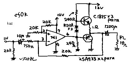
See upper side of the figure! It is called the pure-complementally-push-pull-amplifier.
I made it and the maximum power of it was 110mW. See lower side of figure.
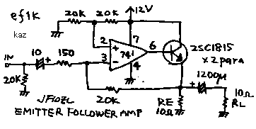
In this circuit, lower side of totem pole (PNP-transistor) is replaced
by the resister. 2SC1815 acts as emitter-follower. Output impedance of
this circuit is decided by the Re-resister. Therefore we must use about
8 ohm Re, in order to use 8 ohm speaker. Power-output of this circuit is
72mW. This circuit needs very big idle-current (=150mA), so it is not power-effective.
But this machine acts as A-class-amplifier; therefore it has no possibility
to make any torsion.
.
ef1k.gif
 僄儈僢僞乕-
僼僅儘傾- 僷儚乕-憹暆婍丏
忋偺恾傪尒偰壓偝偄! 偙偺夞楬偼丆弮僐儞僾儕儊儞僞儖僾僔儏僾儖憹暆婍偲屇偽傟偰偄傑偡丏偙傟傪嶌偭偨偲偙傠丆嵟戝弌椡110mW偑摼傜傟傑偟偨丏壓懁偺恾傪尒偰壓偝偄丏偙偺夞楬偱偼丆僩乕僥儉億乕儖偺壓懁(
PNP僩儔儞僕僗僞乕)偼丆掞峈偵傛偭偰抲偒懼偊傜傟偰偄傑偡丏2俽俠侾815 偼丆僄儈僢僞乕僼僅儘傾偲偟偰摦嶌偟偰偄傑偡丏偙偺夞楬偺弌椡僀儞僺乕僟儞僗偼丆Re偲彂偄偨掞峈偵傛偭偰寛傔傜傟偰偄傑偡丏偦傟備偊偵丆8
僆乕儉僗僺乕僇乕傪巊偆偨傔偵偼丆俼倕偵栺8 僆乕儉傪巊傢側偔偰偼偄偗傑偣傫丏偙偺僒乕僉僢僩偺弌椡揹椡偼丆72mW
偱偡丏偙偺夞楬偼丆偲偰傕戝偒偄傾僀僪儖揹棳( = 150mA ) 偑昁梫偱偡丆偟偨偑偭偰丆偦傟偼丆揹尮偑岠棪揑偱偼偁傝傑偣傫丏偟偐偟丆偙偺婡夿偼A僋儔僗憹暆婍偲偟偰摦嶌偟偰偄傑偡丅偦傟備偊偵丆偙傟偼丆傂偢傒傪惗偠傞壜擻惈偑桳傝傑偣傫丏
add description on 14 feb 98
捛壛婰嵹 侾俋俋俉丏俀丏侾係
ef3.gif

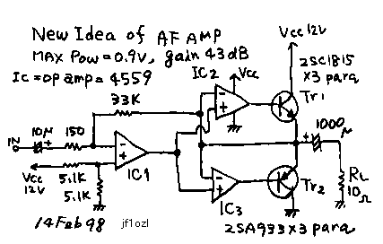
New type of complimentary power amplifier
(It is my idea!)
I will show you my new idea about a complimentary power amplifier. See
the circuit of upside "ef0k"! This circuit has a weak point.
The current of the bias diodes changes, because the voltage on the output
of the driver IC changes. Then the bias voltage has to changes. That makes
a distortion. See the circuit of lower side "ef3"! IC2 and TR1
construct an emitter follower circuit like that of "ef1". IC3
and TR2 also construct an emitter follower. On each circuit, the minus
input of the operational amplifier is connected to the emitter of the transistor;
therefore the emitter's voltage becomes the same voltage from a plus input
of the operational amplifier. Therefore this circuit constructs a linear
current amplifier. The voltage amplification of it is 1 times. IC1 works
as a voltage amplifier. The minus input of it is connected to the output
of the whole circuit. Therefore the whole minus feedback is made by IC1.
The distortion of this circuit is very small. This amplifier has 0.9W power
output. Frequency characteristic is very flat from 333Hz to 24 kHz. It
is my idea. But I am only amateur of electronics. I did not make any survey
about patent of this circuit.
僯儏乕僞僀僾偺僐儞僾儕儊儞僞儕乕憹暆婍乮巹偺傾僀僨傾偱偡丅乯
忋偺恾乮EF0K乯偵帵偝傟偨丄椙偔抦傜傟偨僐儞儞僾儕儊儞僞儕乕僷儚乕傾儞僾傪婎偵丄怴偟偄夞楬傪峫埬偟偨偺偱丄徯夘偟傑偡丅俤俥侽俲偺夞楬偱偼丄僩儔
儞僕僗僞乕偺僶僀傾僗晹暘偵夞楬忋偺寚揰偑偁傝傑偡丅俈係侾俬俠偺俇斣僺儞偺揹埑偑曄壔偡傞偲丄擇屄偺僶僀傾僗僟僀僆乕僪偵棳傟傞揹棳傕曄壔偟偰丄寢壥揑
偵僶僀傾僗揹埑偑曄摦偟偰偟傑偄傑偡丅忋偺恾偱偼丄偙偺塭嬁傪寉尭偡傞偨傔偵丄擇屄偺僟僀僆乕僪偵俀俀mA傕偺揹棳傪棳偟偰偄傑偡丅偙偙偺強偵俥俤俿傪
巊偭偨掕揹棳夞楬傪巊偆椺傕嶨帍偵傒傜傟傑偡偑丄偪傚偭偲僗儅乕僩偱側偄丅偝偰丄俤俥俁偺恾傪偛棗偔偩偝偄丅俬俠俀偲俿俼侾偼丄恀傫拞偺俤俥俀偺恾偲摨偠
僄儈僢僞乕僼僅儘傾乕夞楬傪宍惉偟偰偄傑偡丅俬俠俁偲俿俼俀偼摨偠夞楬傪俹俶俹僩儔儞僕僗僞乕偱嶌偭偰丄揹尮偲傾乕僗傪媡揮偟偨夞楬偱偡丅乮惓捈偄偭偰丄
巹傕丄恀嬻娗偐傜擖偭偨暔偱偡偐傜丄偙偺丄俹俶俹僩儔儞僕僗僞乕偺儅僀僫僗偑揹尮偲偄偆傗偮偵偼丄傑偝偵揤抧媡揮偺姶偑偁傝丄側偐側偐偮偄偰偄偗傑偣傫偱
偟偨丅乯偦傟偧傟偺擇偮偺僄儈僢僞乕僼僅儘儚乕夞楬偼丄弌椡僩儔儞僕僗僞乕偺僄儈僢僞乕偐傜丄僆儁傾儞僾偺儅僀僫僗抂巕偵僼傿乕僪僶僢僋儖乕僾偑宍惉偝傟
偰偄傞偺偱丄寢壥偲偟偰丄僄儈僢僞偺揹埵偼俬俠偺僾儔僗擖椡抂巕偺揹埵偵摍偟偔側傝傑偡丅傛偭偰丄俬俠俀偲俬俠俁偺擖椡傪偮側偄偱傗傞偲丄偙偙傪擖椡偲偟
偨丄揹埑憹暆棪偑侾攞偺揹棳憹暆婍偑弌棃傞栿偱偡丅偁偲偼丄俬俠侾偵傛偭偰丄晛捠偺扨揹尮偺斀揮憹暆婍傪偮偔偭偰傗傝丄偙傟偵傕偆堦搙慡懱揑側晧婣娨傪偐
偗偰丄榗傒傪掅尭偟偰偄傑偡丅幚嵺偵嶌偭偰傒傞偲丄峫偊捠傝偁偭偗側偔嶌摦偟傑偟偨丅幚應嵟戝柍榗傒弌椡侽丏俋倂偲侾俀倁揹尮偲偟偰偼忋弌棃偱偡丅側偵偟
傠丄偙偺夞楬偵偼丄帪掕悢傪帩偮晹暘偑擖椡偺僐儞僨儞僒乕偔傜偄偟偐偁傝傑偣傫偐傜丄慡懱偑僆儁傾儞僾傒偨偄側傕偺偱丄廃攇悢摿惈偼俁俁俁俫倸偐傜丄
俀俁俲俫倸傑偱姰慡偵僼儔僢僩偱偟偨丅巹偼僨儏傾儖僆儁傾儞僾偺俠倃俙係俆俆俋俹乮僜僯乕惢乯傪擇屄巊偄傑偟偨偑丄扨揹尮梡偺僋儚僢僪傪巊偊偽丄戝曄僗
儅乕僩偵婎斅壔弌棃傞偲巚偄傑偡丅壗偟傠柍挷惍偱丄晹昳傕慖傃傑偣傫偐傜丄椙偄夞楬偩偲巚偄傑偡偑丄偄偐偑偱偟傚偆丅
--------------------------------------------------------
I would like for you to put my mail on your home page. I am attaching the
amplifier schematic in gif format this time in hopes that you can read
it. Again, thanks for putting up such a great page. Best Regards, Ray Given
AB0Hz -----Original Message----- From: [email protected] [SMTP:[email protected]]
Sent: Saturday, December 11, 1999 6:39 AM To: 'Ray Given' Subject: RE:
Dear Ray. Thanks your letter. I want to up your mail on my home page. Please
agree it. Please send me what you send me with gif or bmp! I can not deal
tiff. Kaz ---------- From: Ray Given[SMTP:[email protected]] Sent:
Saturday, December 11, 1999 5:39 To: '[email protected]'<< (J L'2Y
: Aud_AMP.tiff>>Dear Kazuhiro, (J I want to thank you for putting
up such a wonderful web site. I am a radio amateur and enjoy building equipment
myself. I have spent many wonderful hours looking at your designs and contemplating
my own. I particularly want to thank you for the idea on building an audio
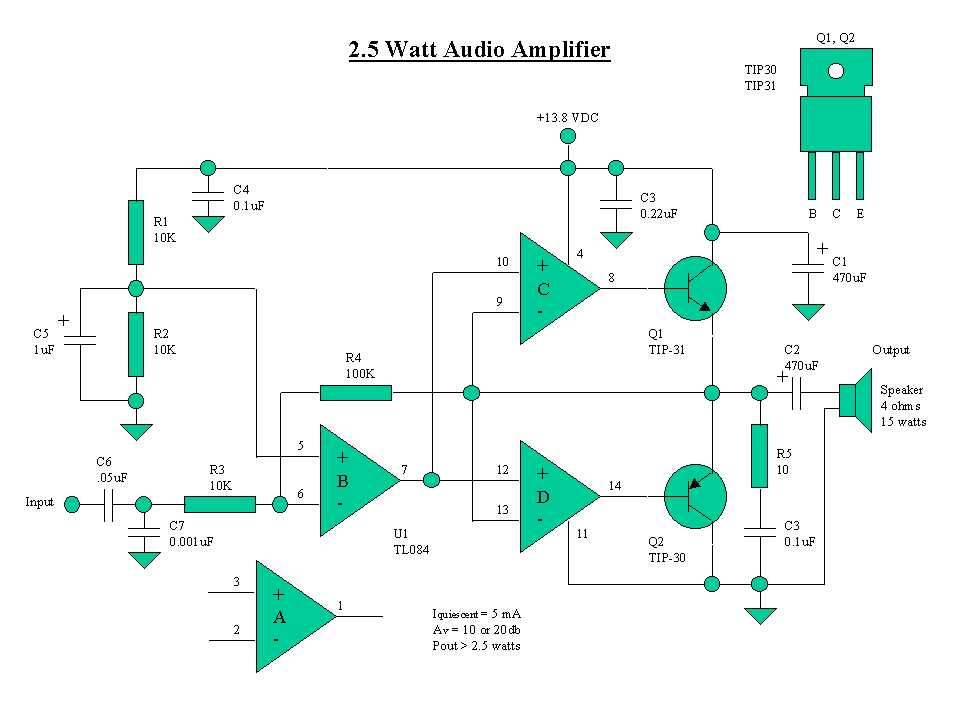
amplifier using a Quad Op Amp and two power transistors. I am attaching
a schematic of my finished amplifier. It will drive a 4 ohm/15watt computer
speaker at 2.5 watts and sounds great. It works extremely well and will
be a standard building block for my future projects needing an audio amplifier.
It also provides one extra Op Amp to do additional filtering if necessary.
The minor circuit changes insured stable operation with out oscillation.
I have attached a copy of the schematic in tif format. 73 Ray Given AB0Hz
ef4.gif
捛婰丗侾俀俢俤們俋俋丗儗僀偝傫偐傜丄巹偺夞楬傪傾儗儞僕偟偰俀丅俆倂偺傾儞僾傪嶌偭偨丅夣揔丅偲偺偍曋傝傪偄偨偩偒丄摨帪偵夞楬恾傪偍傛偣偄偨偩偒傑偟偨偺偱丄忋偵徯夘偟傑偡丅
return to index

 Emitter-follower-power-amplifier.
 僄儈僢僞乕-
僼僅儘傾- 僷儚乕-憹暆婍丏